Application specific trade-offs between WBG SIC, GaN, and high-end SI power switch technology
Faced with the ever-changing semiconductor technology, SiC FET (MOSFET) and transverse GaN HEMT are still one of the most important devices in power switching technology. With the latest developments in this field, SiC and GaN have played a significant role in improving the performance of power devices and high-power application circuits. In addition, these devices exhibit higher efficiency while significantly reducing production and implementation costs.
SiC FET (MOSFET) and transverse GaN HEMT are two components that have achieved significant success in the field of power semiconductors. Compared to traditional SiC wafers, GaN wafers can operate in similar environments with significantly lower failure rates in terms of durability and voltage derating. All power semiconductor devices operate at voltages between 600 and 1200 volts, therefore devices based on SiC and GaN (such as JFET,...) The performance of MOSFETs and IGBTs has been greatly improved within this voltage range.
一、The competitive situation of power switching devices

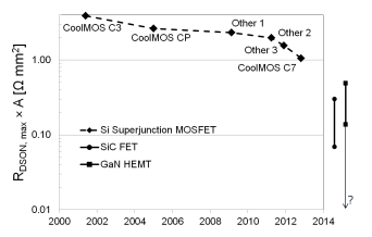
Figure 1 shows the development trend of xA in RDS.
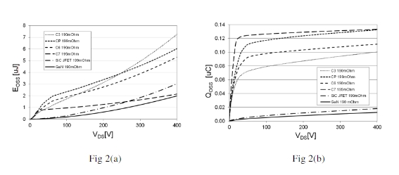
Figure 1 shows the conduction resistance value between the drain and source (RDS, on), Suitable for various MOSFETs, including Infineon CoolMOS series MOSFETs. The modern SiC switch concept is expected to reduce the conduction resistance by five times, but unfortunately, this is consumed by the high SiC area cost of 650V devices. The ideal conduction resistance value is 1 Ω mm ², and to achieve this value, the unit spacing is reduced by compensating for accuracy. Observations during the experiment indicate that the energy or Eoss value stored in the output capacitor of the recently developed device has been reduced by half, making it closer to the values of SiC and GaN.
二. Insulated gate bipolar transistor
The power density of IGBTs with a rated voltage of 650V-1700V is being improved and upgraded to enhance efficiency by utilizing local plasma density. In many cases, these devices are suppressed by high currents and related low short-circuit effectiveness. This seems to be a limitation, but it can be solved by appropriate diffusion welding, sintering, and thicker positive power metal as temporary heat sinks. Another drawback of IGBT is the lack of integrated freewheeling diodes, which means that the reverse conduction voltage is zero. Therefore, IGBT always outperforms all other power switch technologies. Unfortunately, despite various improvements currently available, the switch loss provided by WBG switches is only 1/10, provided that the dV/it is high and the assembly setting inductance is small.

Figure 2 (a) Comparison of output capacitor storage energy. Figure 2 (b) Comparison of stored charges in output capacitors
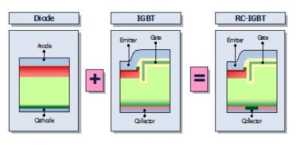
In addition, all IGBT losses are bipolar, and due to the continuous increase of minority carriers, such devices are related to T. This can lead to an increase of up to 40-50% in temperature issues. In addition, reverse conduction IGBT is considered an active gate control that can reduce minority carrier density before turning off the diode. Therefore, this benefit depends on the ratio between static and dynamic losses, which may be the dI/dt or dv/dt gradient.
Ⅲ. SiC FET

Figure 3 IGBT reverse conduction using freewheeling diodes
四、GaN HEMT
GaN (gallium nitride) has greater advantages than SiC, but it is also a material that is more difficult to crystallize and process than SiC. HEMT technology only forms components on the substrate surface of GaN crystals. The difference between GaN HEMTs and other HEMTs is that their gate is very low, with zero recovery loss, and they exhibit destructive breakdown rather than avalanche in other devices. These devices are grown on n-heteroepitaxial materials with low Rds and can achieve high current density, but they are hindered by low heat capacity. The switching losses that occur in GaN HEMT are temperature independent, as they are purely capacitance losses similar to MOSFETs. There is a risk of thermal runaway in GaN HEMT, which can cause damage and potentially short circuits. This is completely consumed in the drive, and PFC occurs after the AC power is cut off.
五、Conclusion

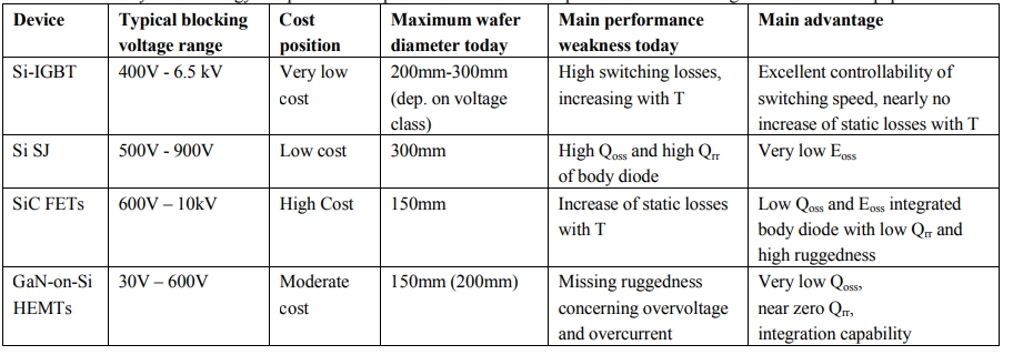
Figure 4 Analysis of related technologies and performance parameters of power switch technology
The above table displays various devices, their voltage ranges, and their respective properties.
SiC based IGBT is considered the best device in the high voltage range of 400V-6.5kV, while GaN on Si HEMT is considered the best device in the high voltage range of 400V-6.5kV. Considering this, GaN on Si HEMT is considered an ideal choice for the voltage range of 30V-600V. If cost standards are not considered, SiC devices have the upper hand in all aspects. The advantage of SiC based devices is that they can operate within a high voltage range without losing their blocking ability.
Initially, this was because cheaper GaN substrates with larger diameters (150mm and 200mm) could be purchased. Then, GaN can be extended to higher voltage levels above 650V, thereby reaching the limits of SJ and IGBT technology. There are many methods to improve the productivity of equipment, but due to increased manufacturing costs, the challenge is the feasibility of these methods. Overall, the prices of devices are becoming increasingly competitive, and the importance of uniqueness for specific applications of devices is increasing. In order to improve the efficiency and reliability of power devices, it is necessary to conduct more research and development on various materials used in power semiconductor technology.
