Development of Ga2O3 semiconductor materials with ultra wide bandgap in power MOSFETs
Power electronics technology is currently under development, aiming to achieve efficient power conversion of electricity through static means, thereby achieving energy conservation directly related to the performance of power devices. People have systematically studied wide bandgap (WBG) materials such as SiC and GaN to achieve high operating voltage and energy conversion efficiency. It improves the power density and efficiency of power electronic systems. Further development requires consideration of several advanced improvements, such as high breakdown voltage, low energy loss, low-cost, and easily integrated cutting-edge semiconductor technologies.
Despite the increasing number of papers on Ga2O3, the progress and performance of beta Ga2O3 still lag behind SiC and GaN. Behind every power application, metal oxide semiconductor field-effect transistors (MOSFETs) are the most important component.
The basic properties of gallium oxide:
1) The crystal structure of Ga2O3:
Corundum( α) And monoclinic( β) It is the most commonly used homogeneous variant of Ga2O3 single crystal. There are also other homogenous isomers, such as defective spinel( γ) And rhombic( ε), Among them δ Phase is widely regarded as a form of rhombic phase.
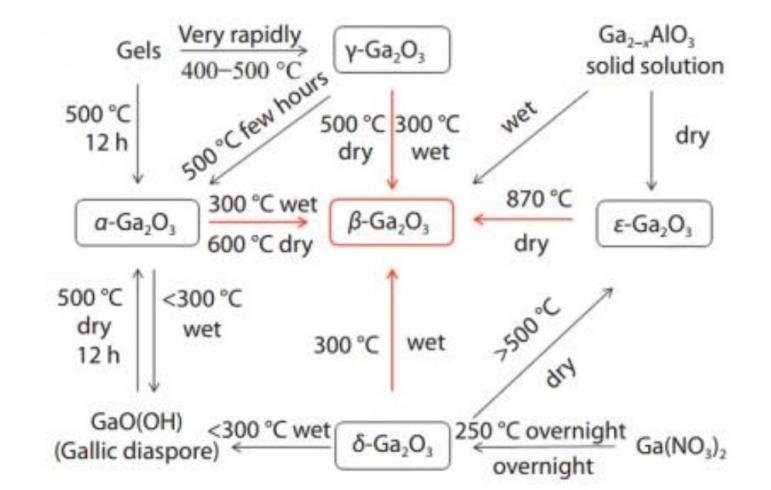
Figure 1. (a) Figure 1. (b)
In Figure 1 (a), all phases of Ga2O3 can remain stable at room temperature and transform into other phases at high temperature or pressure, with the most stable being the monoclinic phase of Ga2O3( β- Ga2O3).
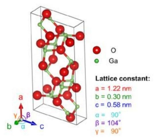
Gallium (Ga) atoms exist only in two forms: tetraligands and hexaligands, as shown in Figure 1 (b). β- The Ga2O3 crystal structure is stacked with [GaO6] octahedra and twisted [GaO4] tetrahedra, respectively. Physical and optical properties, such as different thermal conductivity at (-201), (100), and (010) due to the different positions of Ga and O atoms
2) β- Physical properties of Ga2O3:
Table 1 lists some important physical properties of semiconductors, among which β- The highest thermal conductivity of Ga2O3 is 0.27 W cm-1 K-1, and the lowest thermal conductivity is 0.1-0.3 W cm-1 K-1. Various semiconductors can be compared using different coefficients of performance (FOM).
In addition to p-type doping, thermal conductivity is also another issue for the power application of β - Ga2O3, as shown in Table 1. Therefore, people believe that as long as the disadvantage of poor thermal conductivity, β - Ga2O3 will maximize its potential in unipolar power devices.
3) Single crystal Ga2O3:
Manufacturing electronic devices suitable for high voltage and high-power applications typically requires large area, low defect density crystals. The melt growth method is highly likely to achieve low-cost commercial substrates, and compared to other WBG SiCs Compared to semiconductors such as diamond, AIN's economic competitive advantage is emerging.
Edge limited film feeding (EFG) is a widely used method for producing Ba2O3 crystals. There are other methods, such as floating zone (FZ) and vertical Bridgman (VB) growth.
Manufacturing process of Ga2O3FET:
i) Gate dielectric and surface passivation on Ga2O3 devices:
Effective gate control capability is crucial for the performance of Ga2O3 based MOS devices and must meet the following prerequisites. Firstly, the gate dielectric must not react during the processing and have thermodynamic stability with the semiconductor. High channel mobility, interface quality, and defect density are also required. Finally, the energy band offset of the gate dielectric/Ga2O3 is discussed as one of the key parameters, and a suitable gate dielectric must have sufficient energy band offset (conduction band offset and valence band offset are usually greater than 1 eV) to act as electron or hole barriers, respectively.
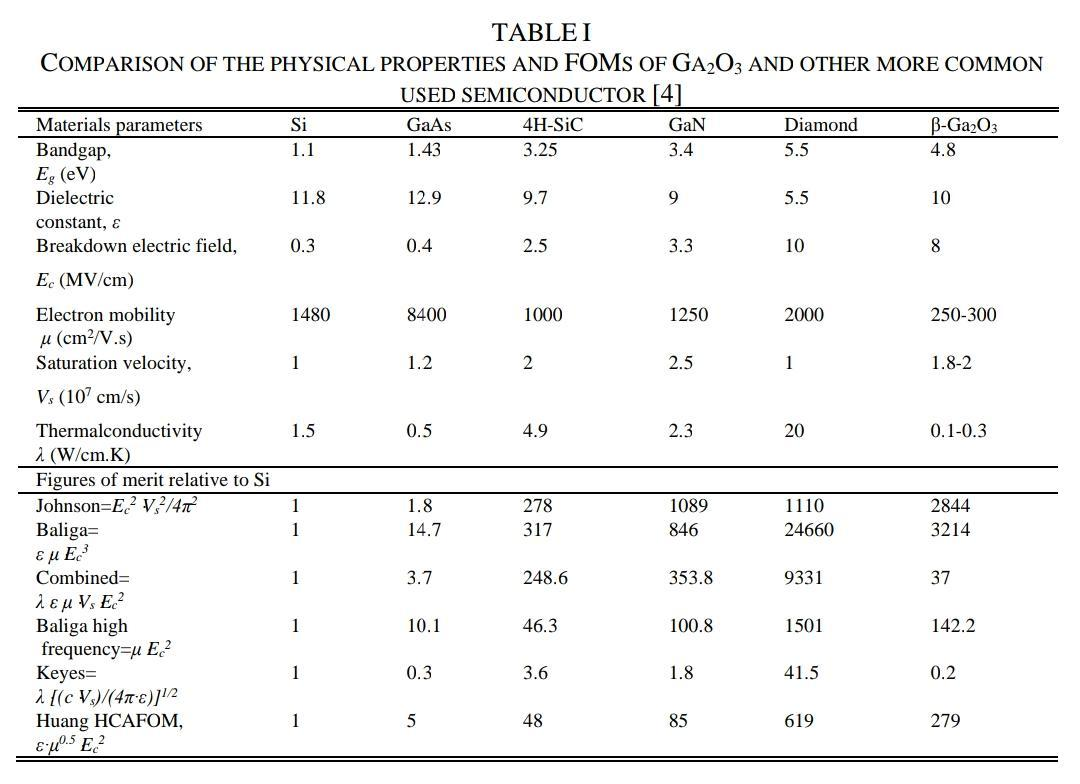
Table II summarizes the band offset and band arrangement types extracted from various dielectrics deposited on Ga2O3 or AlxGa1-xO as reported.
Ii) Contact and etching on Ga 2O 3:
It is important to obtain reliable ohmic contacts with low specific contact resistance and suitable high temperature in order to reduce the power loss and specific on resistance (Ron) of the device. Doping Si ions in Ga2O3/Ti/Au helps to achieve Ohmic contacts with low specific resistance, with resistivities of 4.6 × 10⁻⁶ Ω. cm2 and 1.4 m Ω. cm. Donor ions such as Sn and Ge are also used for ion implantation to form the drain/source electrodes of Ga2O3 MOSFETs.
The patterned structure and isolation devices of Ga2O3 mainly adopt wet etching and dry etching processes. The quality of the crystal determines the rate of wet etching. At room temperature, HF and HCl solutions have better etching effects on Ga2O3; At high temperatures, solutions such as H3PO4, KOH, and H2SO4 are used for wet etching of Ga2O3. Dry etching of Ga2O3 can achieve higher resolution patterning processes Dry etching uses high-density plasma etching techniques such as electron cyclotron resonance (ECR, operating frequency 2.45 GHz), inductively coupled plasma (ICP, operating frequency 2-13.56 MHz), and reactive ion etching (RIE). For β- The chloride based dry etching of Ga2O3 is superior to RIE due to its high plasma density and considering the etching rate and surface roughness.
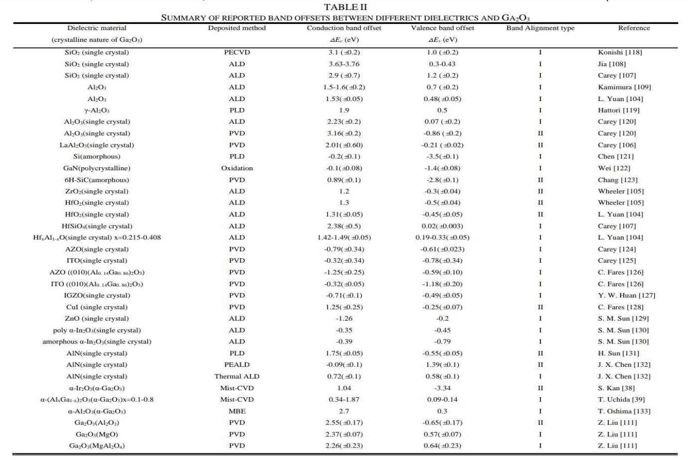
Figure 2 (a) The relationship between the etching rate of β - Ga2O3 and the Cl2 content in Cl2/BCl3 ICP plasma [161]; (b) The relationship between the etching rate of BCl3/Ar and Cl2/Ar ICP etching and substrate temperature [161]. (c) The relationship between the etching rate of UID (-201) β - Ga2O3 and the RIE power at different ICP powers [160]; (d) The relationship between etching rate and ICP power at 60W RIE power [160]
Overview of Ga 2O 3 MOSFET:
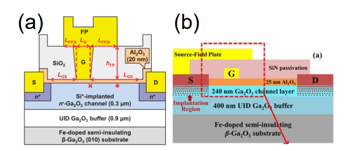
MH Wong et al. used Si+ion implantation doping method to fabricate Ga2O3 fieldboard MOSFETs (FP MOSFETs) consisting of gate connected fieldboards and chemical vapor deposition (CVD) SiO2 passivation layers. The breakdown voltage in the off state is 755 V, the current on/off ratio is above 109, and it can maintain stable high-temperature operation under thermal stress of 300 ° C.
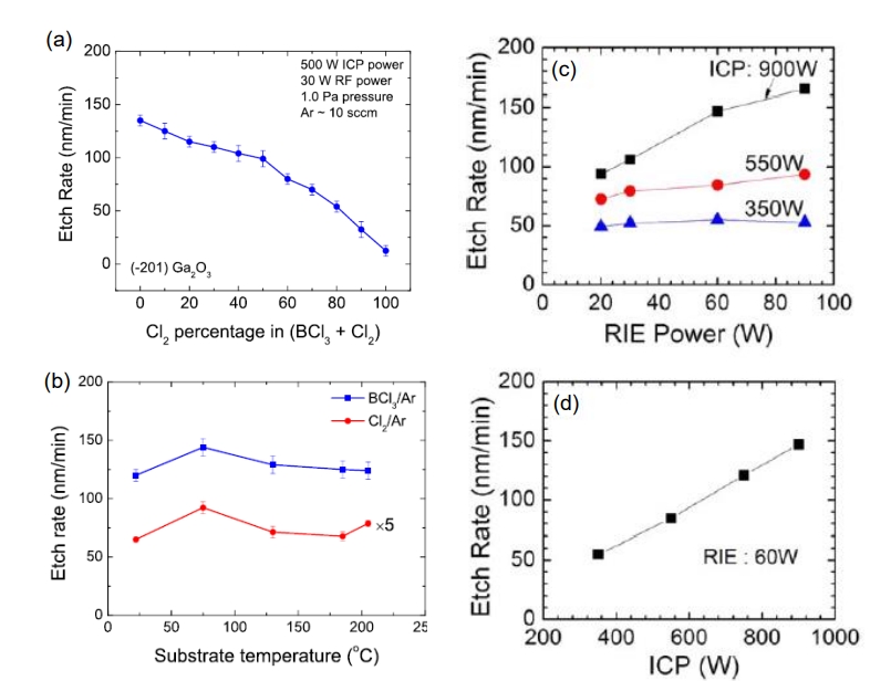
Figure 3 (a) Schematic Cross Section of General Ga2O3 FP-MOSFET [22], (b) Schematic Cross Section of Source Connection FP-MOSFET [23]
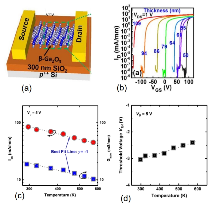
One method is to reduce the thickness of the channel to ensure that it is completely depleted below zero Vgs, including on the insulator β- Ga2O3 field-effect transistor (GOOI FET) [17], [136], [137]. Another method is to use a thin active region to completely deplete the channel at zero gate bias (Vgs), which also includes modulation of channel doping concentration (Nd) and gate metal work function( Ф m)
Interface charge (Qit) at the interface with oxide/Ga2O3.
Figure 4 (a) Schematic diagram of GOOI FET (b) Thickness related ID-Vgs diagrams for various GOOI FETs from D mode to E mode [17]. (c) Temperature dependent characteristics of ION and peak Gm, int [183] and (d) on AlN/Si substrates β- Vth temperature dependence of Ga2O3 GOOI FET
The main challenges facing the development of Ga2O3 are the development of effective shallow acceptors and effective Ga2O3 p-type doping technology, as well as the severe self heating effect caused by the ultra-low thermal conductivity (κ) of Ga2O3. These issues can be addressed by considering the following points:
Develop large-diameter, high-quality single crystals.
● Epitaxial growth.
● E-mode operation
● Thermally stable Schottky contacts.
● Process optimization.
● Gate modulation of transistors.
● Reduce RON.
● Modeling and device simulation in Ga2O3.
● Equipment reliability and future analysis (FA).
● Thermal management.
Table 3
Power electronic devices are used for motor control, photovoltaic inverters, electric vehicle drives, rail transit, ships, windmills, and smart grids to convert energy in power systems. Nowadays, devices based on Si and SiC dominate the high-voltage/high-power market, while ultra wideband gap (UWBG) materials such as Ga2O3 and diamond are considered to be potentially used in the high-power market (>1 kW). Gas sensors and day blind photodetectors are applications of gallium (III) oxide [Ga2O3] semiconductors.
Conclusion:
In the past few years, Significant progress has been made in the development of β - Ga2O3 single crystals and thin films. Researchers have demonstrated several effective solutions to address the issue of p-type doping deficiency, including low doping channels, high work function gate metals, vertically moderately doped fins, thin channel geometries using gate groove processes GOOI FET structure and thin depletion layer of gate region interface states. More research is needed on p-type doping and device manufacturing. It is necessary to develop β - Ga2O3 FETs for power applications and reduce the gate length for high-frequency applications. After solving the above problems, it is expected that Ga2O3 devices will compete with mid to high power Si and SiC devices.
